| FPGA
About
About
Contact Us
Contact Us
GitHub
GitHub
(opens in a new tab)
On This Page
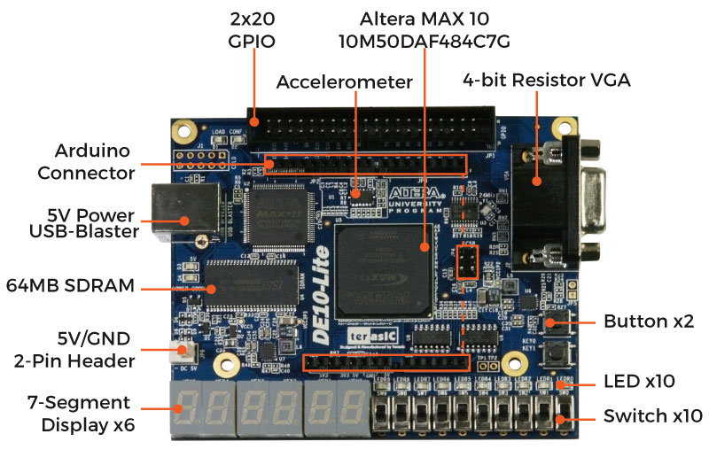
Layout and Components
Question? Give us feedback →
(opens in a new tab)
Edit this page
DE10-Lite
Layout and Components
Layout and Components
Lab Overview
Installation